
Power Electronics Insights — a PA International technical series
Copper weight is one of the first numbers on a PCB fabrication drawing, and one of the least discussed in the design review. It gets picked early — often by habit, by copying the last design, or by a fab house default — and by the time a board comes back hot or a trace lifts during rework, the decision is long buried. It shouldn’t be. Copper weight sets how much current a trace can carry, how far it can run before the voltage drop matters, how fine a pitch the fabricator can etch, and a meaningful share of the unit cost.
What copper weight actually controls
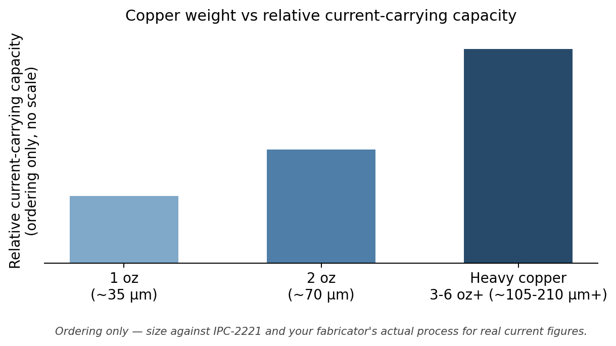
“1 oz copper” means one ounce of copper rolled out over one square foot of board, which works out to roughly 35 µm of thickness; 2 oz is about 70 µm; heavy copper conventionally starts around 3 oz (~105 µm) and runs up past 6 oz (~210 µm) for the most demanding power boards. Thickness is the whole story for current-carrying capacity: a wider or thicker trace has more cross-sectional area, so it can carry more current for the same temperature rise. The standard reference for this trade-off is IPC-2221’s external-layer current-capacity charts, and any real design should be sized against those curves and the fabricator’s actual etch tolerances — not against a rule of thumb copied from a different board.
Thicker copper also changes how the board is made. Etching is a subtractive process: acid removes copper from around the traces you want to keep, and it attacks sideways as well as down. That sideways attack — undercut — is proportional to copper thickness, so a fabricator etching 1 oz copper can hold much finer trace and space than one etching 6 oz copper on the same line. This is the reason “just make it thicker copper” is not a free upgrade: it costs you minimum trace width, minimum spacing, and often layer count once you need fine-pitch signal routing alongside the power section.
Copper weight at a glance
| Copper weight | Typical thickness | Where it’s used | Fabrication impact | Relative cost / lead-time |
|---|---|---|---|---|
| 1 oz (~35 µm) | Standard | Signal and low-current logic boards, most control circuitry | Finest achievable trace/space, standard etch process | Baseline |
| 2 oz (~70 µm) | Moderate | Mixed power/signal boards, moderate-current power supplies | Noticeably coarser minimum trace/space than 1 oz; still a common stocked process | Modest increase |
| Heavy copper, 3–6 oz+ (~105–210 µm+) | High-current | Power converters, motor drives, battery management, busbars-on-PCB | Requires pulse plating and controlled undercut compensation; wider minimum trace/space; longer lead time | Meaningful increase, more so at higher layer count |
Treat this as an ordering, not a specification — always confirm minimum trace/space and current-capacity figures against your fabricator’s current process capability and against IPC-2221 for your actual current and temperature-rise targets.
Design-rule consequences that follow the choice
Two consequences matter more than most designers expect. First, the etch factor — the ratio of vertical to lateral etch — degrades as copper gets thicker, which means a trace drawn at, say, 0.2 mm on a 1 oz layer may come back narrower than intended at 4 oz unless the fabricator’s undercut compensation is built into the artwork. Second, via aspect ratio: plating a via wall evenly gets harder as copper thickness (and often board thickness, on a heavy-copper power layer) increases, so heavy-copper boards frequently need larger minimum via diameters or additional plating steps to hit reliable barrel thickness. Both are things a fabricator should flag at DFM review — but only if the copper weight and the current targets are stated on the drawing, not left implicit.
When heavy copper is justified — and when it’s just cost
Heavy copper earns its keep when a design genuinely needs to move tens of amps through a compact board: our earlier note on designing PCBs for GaN and SiC power stages covers a case where primary-side currents reach 80–100 A RMS and 3–6 oz outer-layer copper is the practical answer, because the alternative — much wider traces on 1 oz copper — simply doesn’t fit the board outline. At lower currents, though, heavy copper is a straightforward net cost: it buys current margin the design doesn’t use while giving up fine-pitch routing the design does need. The honest sizing exercise is to work out the actual current path, apply IPC-2221 (or a validated thermal model) for your acceptable temperature rise, and pick the thinnest copper that clears that number with reasonable margin — not the thickest copper “to be safe.”
There is also a middle path worth knowing about: selective or stepped copper, where heavy copper is used only in the specific power zone and a lighter weight elsewhere on the same layer. It costs more in process complexity than a uniform weight but can avoid forcing the whole board — including the fine-pitch control section — onto a coarse-etch process. If your board mixes a genuine current-carrying section with dense low-current logic, this is worth raising with the fabricator at quote stage rather than discovering after the first prototype run.
What to put on the RFQ
A copper-weight decision only helps if it survives translation to a manufacturable drawing. State the copper weight per layer, not just “heavy copper” — inner and outer layers are frequently different weights on the same board. State the current and expected temperature rise per critical trace, not just the copper weight, so the fabricator’s DFM review can catch a mismatch before tooling. And if the board also needs IMS or metal-core construction because the heat has nowhere else to go, say so up front — copper weight and substrate choice are usually solved together, not in sequence. Rigid-flex sections carrying heavy copper are a further special case, since the flex region typically needs a different, thinner copper weight than the rigid power section.
Getting the copper weight the design actually needs
This is a decision PA International’s manufacturing partners deal with on every current-carrying board that reaches them. Through its network of specialist fabrication partners, PA supplies 1 oz through heavy-copper (6 oz+) constructions, including selective/stepped copper and heavy-copper combined with IMS or rigid-flex sections, with pulse-plating and controlled-undercut processes built for the thicker end of that range. The same partner lines that hold ±10% trace tolerance on 6 oz copper for heavy-copper power PCBs apply that discipline whether the design needs 2 oz or 6 oz — the point is matching the copper to the current, not defaulting to the thickest option available.
If the board also carries a current-sensing element, our companion guide on choosing a current-sensing method covers the same shunt-vs-CT-vs-Hall trade-off from the sensing side.
If you’re sizing copper weight for a new power board — or inheriting a design where nobody remembers why it was specified the way it was — send us the current path and the temperature-rise budget, and we’ll tell you the copper weight (and the trace geometry) it actually needs. Get in touch to scope a current-carrying PCB.
Power Electronics Insights is PA International’s technical series for power-electronics engineers. Technical reference only; current-capacity and process figures are aggregated from IPC-2221 industry guidance and PA International’s manufacturing-partner programme.