
Power Electronics Insights — a PA International technical series
GaN gets the headlines. The PCB underneath it does not — but it decides whether the design works.
Wide-bandgap devices — gallium nitride and silicon carbide — earn their reputation by switching hard and fast. A modern GaN totem-pole PFC stage eliminates the diode bridge that used to dissipate 1–2% of throughput power on its own, and pushes measured stage efficiencies above 98–99% in optimised designs. But those numbers come with a condition attached: switching edges compressed into the 10–20 ns range, at which point parasitic inductance that was once negligible becomes first-order. A few nanohenries in the gate-drive loop produce overshoot and ringing on the gate; the same order of inductance in the power commutation loop generates drain-source spikes that can exceed device ratings or radiate broadband EMI.
In this regime the PCB is no longer a passive carrier for components. Its copper pours, via placement and layer stack-up directly determine loop inductance, thermal resistance and common-mode noise paths. The board is part of the circuit — and the fabricator is part of the engineering team.
Layout discipline: what the fast edges demand
The design response is not exotic; it is disciplined. Multilayer boards — often six layers or more — with meticulous return-path planning so that high-frequency current loops enclose minimal area. Gate-drive traces routed as tightly coupled pairs or embedded striplines. Decoupling capacitors placed inside the power loop, or on the underside directly opposite the switches. These are not incremental refinements: they are the difference between a working power stage and one that fails radiated emissions or destroys itself on the first hard transient.
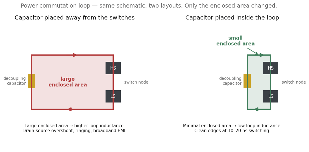
For the fabricator, that layout intent translates into physical tolerances. Controlled impedance has to survive real-world variation in dielectric thickness and copper roughness. Registration between layers has to hold, because a shifted return plane changes the loop geometry the designer counted on. This is why serious power-stage designs increasingly arrive at the fab with the electrical intent spelled out — loop inductance targets called out as explicit constraints, not after-the-fact layout notes.
Copper and current: the heavy-copper power stage
A modern 11–22 kW onboard charger or comparable power-conversion stage packs more than 15 kW into an enclosure smaller than 5 litres, with primary-side currents reaching 80–100 A RMS. The standard answer is heavy-copper power PCBs: 3–6 oz copper on outer layers with 2 oz inner layers for the power section.
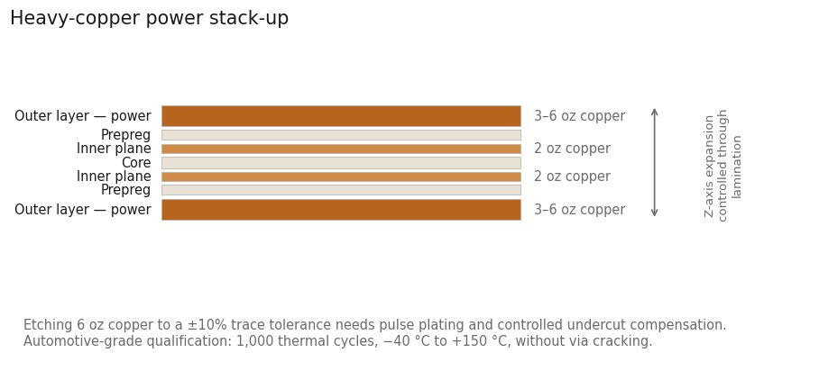
Heavy copper brings its own fabrication physics. Etching 6 oz copper to a ±10% trace tolerance requires pulse plating and controlled undercut compensation — the etchant does not care that the trace width sets your current density margin. Qualification for automotive-grade builds means surviving 1,000 thermal cycles from −40 °C to +150 °C without via cracking, which in turn demands precise control of Z-axis expansion during lamination.
When FR4 runs out: IMS and metal-core substrates
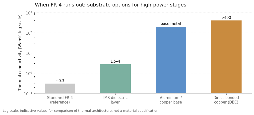
At the highest power densities, heat can no longer be asked to leave through the component side. IMS and metal-core PCBs put an aluminium or copper base under a thin dielectric — 100–200 µm, thermal conductivity 1.5–4 W/m·K — so the board itself becomes the heat spreader, feeding the chassis or a cold plate directly. Premium SiC modules go further, onto direct-bonded copper substrates with effective conductivity above 400 W/m·K. Locally, a GaN half-bridge or synchronous rectifier bank can be dissipating more than 200 W into the board — the substrate choice is not a refinement, it is the thermal architecture.
The same logic extends sideways into the magnetics: planar transformers in these converters are themselves multilayer boards, with thermal vias and copper inlays carrying heat from the core into the substrate. The planar transformer windings and the power PCB are increasingly designed — and manufactured — as one thermal system.
Fewer joints, fewer failures: rigid-flex integration
Vibration-heavy environments punish connectors. Rigid-flex constructions let the control circuitry fold into the same volume as the power stage, eliminating board-to-board harnesses and cutting connector count by 40–60% — fewer failure points, lower assembly cost, and a package that uses the enclosure volume the way the thermal design wants. The fabrication demand shifts to the lamination stack: rigid-flex builds live or die on Z-expansion control through thermal cycling.
Where the harness cannot be designed out entirely, it is worth specifying it as deliberately as the board — see our wiring harness and cable assembly capability.
High voltage raises the bar again
At 800 V, creepage and clearance requirements per IEC 60664-1 dictate minimum trace spacing and coating thickness, and fast voltage slew rates stress insulation in ways older standards never anticipated. Partial-discharge testing at 1.5–2× working voltage is standard practice for 800 V-class designs — a test regime the board construction has to be designed for, not retrofitted to.
The board your simulation promised
This is the gap PA International closes. Through its network of specialist manufacturing partners, PA supplies heavy-copper rigid, IMS/metal-core and rigid-flex PCBs with thermal-via optimisation for high-current power applications. Those partner lines are equipped for the pulse-plating, controlled-undercut etching and Z-expansion control these constructions demand, run thermal-cycle testing on production batches, and support defect rates below 50 ppm on high-reliability power builds.
If your next design leans on GaN or SiC and the layout is starting to matter as much as the BOM, involve the board manufacturer while the stack-up is still negotiable. Send us the constraints your power stage actually has to meet — loop inductance, current density, thermal path, voltage class — and we will tell you what the board needs to be.
Power Electronics Insights is PA International’s technical series for power-electronics engineers. Technical reference only; performance figures are aggregated from publicly available industry data and reference designs (Nexperia, Infineon, Fraunhofer IZM, IEEE publications) and PA International’s manufacturing-partner programme.